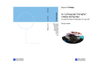
| dc.description.abstract | The aim of this project is to design a small profile, low-power, high performance printed circuit board (PCB) with support for high speed peripherals, while relying on the equipment and facilities of NTNU as much as possible. The intended usage of this module is in image processing applications for autonomous vehicles. The accomplishment of this goal encompasses gaining experience within proficient usage of computer aided design (CAD) tools, implementation of high speed design theory, fabrication of a multilayer PCB, and assembly of advanced components with small footprints and high pin densities, such as ball grid arrays (BGA) and quad flat no leads (QFN) packages. In addition, validation of functionality and testing is also a part of the process.There are several reasons for why such a project is important, and the benefits of carrying out such a project can be leveraged in several areas. First of all, it is desirable to get an overview of the production limitations at the NTNU campus. Where does the limit go for how advanced designs we can produce? What is not possible to do at the NTNU campus? How far can we push our capabilities? Then there is the desire of setting precedence within advanced PCB design and production, in order to build competence at the University that the students and researchers can benefit from in the future. All for the purpose of increasing the quality of their education. Furthermore, low power image processing capabilities with support for high speed peripherals are highly desirable in autonomous vehicles and increase the potential for future research.In order to achieve the goals set for this project, one needs to gain an understanding of what the various components require in terms of design and assembly, and an overview needs to be worked out in order to see how much of these requirements can be met at campus. The process started at finding the correct CAD tool. An attempt was made at using the OrCAD package which The Department of Cybernetics had licenses for. It was discovered that the OrCAD licenses we were in possession of were not suited for the requirements of high-speed bus design. Therefore, an Altium Designer license was borrowed from The Department of Electronics and Telecommunication (IET). Extensive research was done to acquire knowledge about high-speed bus design, which resulted in successful DDR2, Ethernet, and USB bus implementations. The finished design was given the name textit{KybMo}. The workshop at The Department of Engineering cybernetics is in possession of a milling machine for PCB fabrication. However, this machine can only accommodate fabrication of two layer boards, and not 8 layers, as the design required. Thus the fabrication of the board had to be outsourced to an external manufacturer. The department of Engineering Cybernetics recently acquired a re-flow oven that can accommodate assembly of surface mount components such as BGAs and QFNs, but the oven had never been used before, so no one possessed any experience on how to operate it. Gaining this experience was therefore important and the oven was used with successful results. Hand soldering of extremely small discrete components on the bottom side of the board was carried out, as well as successful testing of alternative methods such as using a heating plate and a heat gun with extremely low air pressure in order to avoid blowing the components away. Software packages including stand alone examples, and a Linux system configured for reference designs based on the same System on Chip (SoC) utilized by the KybMo, the OMAP-L138, were modified to fit the configuration of the KybMo and was used for validation of functionality. The project resulted in successful fabrication and assembly of a small, low-power, high performance 8 layer PCB, with over two hundred components. All of the high speed buses were validated and the system was successfully able to boot Linux. This proves that it is definitely possible to design and assemble systems of industrial complexity at the NTNU campus. However, the cost was more than expected. In order for student projects such as this one to be economically supported by the Department, an effort has to be made to push the limits of the design so that less than eight PCB layers are required. Otherwise, an attempt at acquiring external sponsorship is instrumental. | nb_NO |

