| dc.contributor.author | Nilsen, Tron Arne | |
| dc.contributor.author | Breivik, Magnus | |
| dc.contributor.author | Selvig, Espen | |
| dc.contributor.author | Fimland, Bjørn-Ove | |
| dc.date.accessioned | 2017-11-08T09:59:44Z | |
| dc.date.available | 2017-11-08T09:59:44Z | |
| dc.date.created | 2009-03-27T19:11:12Z | |
| dc.date.issued | 2009 | |
| dc.identifier.citation | Journal of Crystal Growth. 2009, 311 (7), 1688-1691. | nb_NO |
| dc.identifier.issn | 0022-0248 | |
| dc.identifier.uri | http://hdl.handle.net/11250/2464861 | |
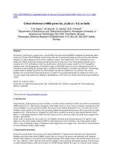
| dc.description.abstract | Several Ga1−xInxSb layers, capped with 1 μm of GaSb, were grown on GaSb(0 0 1) substrates by molecular beam epitaxy in a Varian Gen II Modular system using either the conventional sample growth position with substrate rotation, or a tilted sample position with no substrate rotation. The GaInSb layers were examined by X-ray diffraction (XRD) using both symmetrical and asymmetrical reflections. The “tilted sample method” gave a variation of ±25% in thickness of the Ga1−xInxSb layers, while the indium (In) content varied by ±10% around the nominal value. The disappearance of thickness fringes in 004 XRD scans was used to determine the onset of relaxation, as determining the in-plane lattice constant for tilted samples was found to be difficult. Determining residual strain in samples grown by the tilted method was likewise found to be very difficult. The critical thickness for several In mole fractions between 5% and 19% was determined and was found to be from 2.2 to 2.7 times higher than predicted by Matthews and Blakeslee (1974) [J. Crystal Growth 27 (1974) 118] but lower than that predicted by People and Bean (1985) [Appl. Phys. Lett. 47 (1985) 322]. | nb_NO |
| dc.language.iso | eng | nb_NO |
| dc.publisher | Elsevier | nb_NO |
| dc.rights | Attribution-NonCommercial-NoDerivatives 4.0 Internasjonal | * |
| dc.rights.uri | http://creativecommons.org/licenses/by-nc-nd/4.0/deed.no | * |
| dc.title | Critical thickness of MBE-grown Ga1-xInxSb (x < 0.2) on GaSb | nb_NO |
| dc.type | Journal article | nb_NO |
| dc.type | Peer reviewed | nb_NO |
| dc.description.version | acceptedVersion | nb_NO |
| dc.source.pagenumber | 1688-1691 | nb_NO |
| dc.source.volume | 311 | nb_NO |
| dc.source.journal | Journal of Crystal Growth | nb_NO |
| dc.source.issue | 7 | nb_NO |
| dc.identifier.doi | 10.1016/j.jcrysgro.2008.11.083 | |
| dc.identifier.cristin | 356058 | |
| dc.relation.project | Norges forskningsråd: 177610 | nb_NO |
| dc.description.localcode | © 2008. This is the authors’ accepted and refereed manuscript to the article. This manuscript version is made available under the CC-BY-NC-ND 4.0 license http://creativecommons.org/licenses/by-nc-nd/4.0/ | nb_NO |
| cristin.unitcode | 194,63,35,0 | |
| cristin.unitname | Institutt for elektroniske systemer | |
| cristin.ispublished | true | |
| cristin.fulltext | postprint | |
| cristin.qualitycode | 1 | |

