| dc.contributor.advisor | Ytterdal, Trond | |
| dc.contributor.author | Lund, Håvard | |
| dc.date.accessioned | 2018-11-05T15:01:20Z | |
| dc.date.available | 2018-11-05T15:01:20Z | |
| dc.date.created | 2006-06-13 | |
| dc.date.issued | 2006 | |
| dc.identifier | ntnudaim:1281 | |
| dc.identifier.uri | http://hdl.handle.net/11250/2571099 | |
| dc.description.abstract | A 90nm CMOS technology has been characterized on the basis of IV and CV measurements. This was feasible by means of a state of the art probe station and measurement instrumentation, capable of measuring current and capacitance in the low fA and fF area respectively. From IV results it was found that the static power consumption is an increasing challenge as the technology is scaled down. The IV measurements also showed the impact from small-channel effects, which was not as prominent as expected. Investigation of literature has resulted in a methodology for accomplishing accurate CV measurements on thin-oxide transistors. By using extraction methods on the capacitance measured, key parameters have been obtained for the CMOS technology. Some of the extracted results suffer however from the choice of test setup. | |
| dc.language | eng | |
| dc.publisher | NTNU | |
| dc.subject | Elektronikk, Krets- og systemkonstruksjon | |
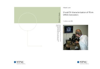
| dc.title | IV and CV characterization of 90nm CMOS transistors | |
| dc.type | Master thesis | |

